
Oxide Electronic Devices for Extreme Operating Environments
NLR leads a collaboration in developing oxide electronic devices for extreme operating environments.
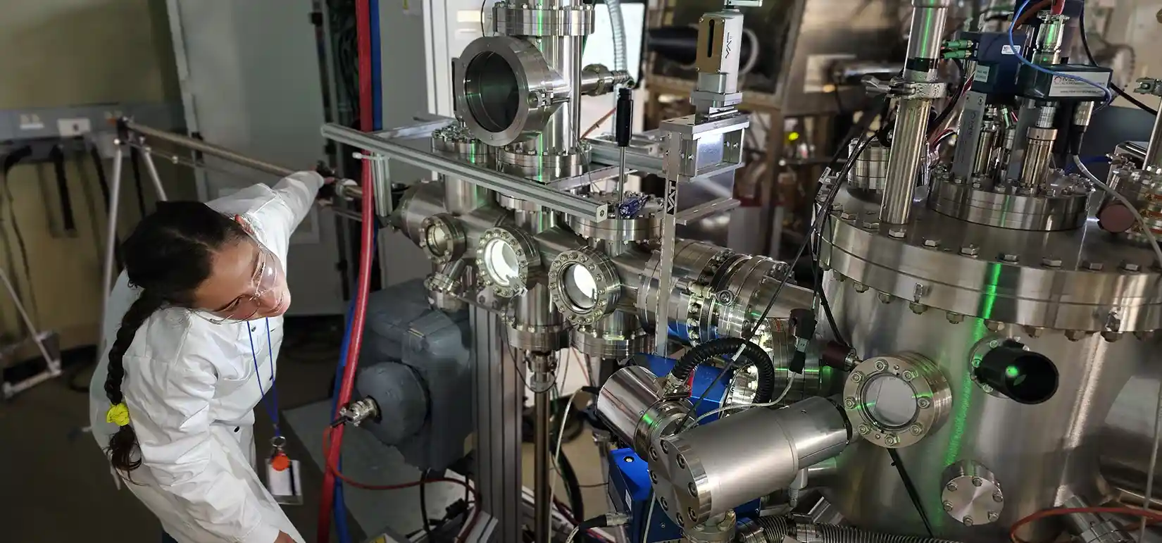
NLR's materials science capabilities are leveraged to advance high-temperature and high-power electronic devices. Photo by Brooks Tellekamp, National Laboratory of the Rockies
Electronic devices that can operate in extreme environments while withstanding electrical, mechanical, thermal, and chemical stresses could significantly advance energy conversion technologies, industrial manufacturing processes, parts of the transportation sector, geothermal down-well monitoring, and mineral extraction and processing. These high-power devices are also relevant to the emerging artificial intelligence (AI) data center industry.
NLR works to demonstrate oxide electronic devices suitable for extreme operating environments, including high-electrical power, elevated temperatures, corrosive atmospheres, and mechanical stresses.
To achieve this goal, the team is:
Improving U.S.-based manufacturing of gallium oxide single-crystal wafers
Depositing high-quality epitaxial semiconductor layers capable of withstanding extreme voltages and temperatures onto U.S.-fabricated wafers
Using the improved wafers to fabricate oxide semiconductor devices and sensors
Evaluating device performance and reliability under extreme conditions.
Compared with established silicon and emerging wide-bandgap semiconductors such as silicon carbide and gallium nitride, high-temperature and high-power gallium oxide electronic devices have the potential for lower costs, better performance, and higher energy efficiency.
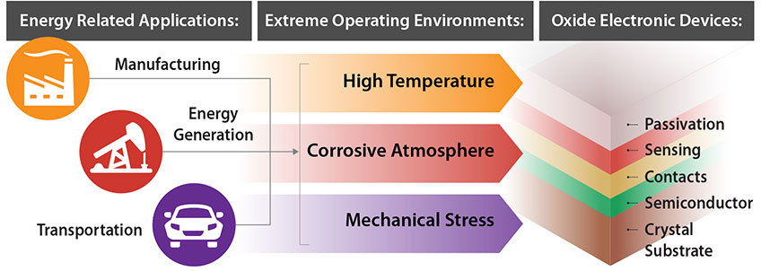
The U.S. Department of Energy's Advanced Materials and Manufacturing Technologies Office provides funding and facilities to support these efforts.
Impact
NLR researchers aim to address technology gaps to make reliable and inexpensive high-temperature and high-power electronic devices for energy-related applications.
This research is increasing the operating temperature and service lifetime of electronic devices such as hydrogen sensors while maintaining performance and reducing manufacturing costs. Researchers are also developing AI-driven methods for accelerated qualification of performance and reliability, demonstrating pathways toward high-voltage electronic devices such as diodes and transistors. Once validated, these electronic devices could improve energy technologies such as aluminum alloy plants, next-generation vehicles, and power delivery to data centers as well as manufacturing processes such as geothermal energy extraction.
Capabilities
Compared to low-power and ambient-temperature applications, extreme operating environments require advanced material manufacturing and processing, device fabrication and characterization, and corresponding measurements and analysis. NLR offers a variety of capabilities to support this work.
Materials
Device
Testing
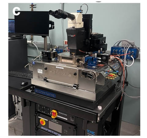
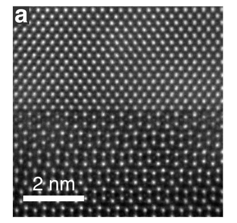
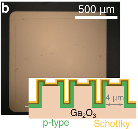
NLR capabilities used in this project include materials synthesis and characterization of atomically precise interfaces; electronic device fabrication and validation shown by top-down view of a trenched microeletronic device; and characterization, modeling, simulation, and AI algorithms illustrated by a high-voltage probe station. Microscopy image of a Ga2O3 interface (a) by Michelle Smeaton, National Laboratory of the Rockies. Graphic by Brooks Tellekamp, National Laboratory of the Rockies
Materials-related capabilities include:
-
Substrate and epitaxial layer fabrication, including halide vapor phase epitaxy (in collaboration with partners), edge-fed single-crystal growth and polishing
-
Thin-film deposition and interface engineering, including molecular beam epitaxy, pulsed laser deposition, sputtering, and atomic layer deposition
-
Materials measurements and characterization, including high-resolution microscopy, correlative microscopy, and secondary ion mass spectrometry.
Device-related capabilities include:
Cleanroom fabrication of diode, transistor, sensor, and other devices
Photolithography, etching, metallization, and dielectric passivation
Probe station electrical testing, including manual, automated, and autonomous systems
High-temperature, controlled-atmosphere, and high-voltage device characterization.
Comprehensive computational simulation capabilities include:
First-principles stability, defect, and interface calculations
Electro-thermal and thermo-mechanical device modeling
Techno-economic analysis of wafer manufacturing cost
Machine learning for accelerated statistical data analysis
AI for equipment automation and measurement autonomy.
Partners
This effort combines knowledge from academia, industry, and national laboratories. Led by NLR with semiconductor materials and electronic device core strengths, the project team includes expertise in high-temperature and corrosive-atmosphere research of the Department of Metallurgical and Materials Engineering at the Colorado School of Mines. Industrial partners include Luxium Technologies Solutions, a company with extensive crystal growth and wafer fabrication facilities, and Kyma Technologies, which specializes in high-rate epitaxial growth processes and equipment.
Projects
These Department of Energy-supported projects contributed to this work:
Pathways to 20-kV Ga2O3 Power Devices (Fiscal Years 2026–2028)
Wide Bandgap Power Electronics Strategic Framework (Fiscal Year 2024–2025)
Accelerated Qualification of Gallium Oxide Semiconductor Gas Sensor Reliability (Fiscal Years 2023–2025)
Oxide Electronic Devices for Extreme Operating Environments (Fiscal Years 2020–2023).
Featured Publications
Autonomous Reliability Qualification of Ga2O3-Based Hydrogen and Temperature Sensors Via Safe Active Learning, arxiv (2026)
Fast Homoepitaxy on (100) Beta-Ga2O3 Substrates With Large Grown-In Offcut, arxiv (2026)
Wide Bandgap Power Electronics Strategic Framework, U.S. Department of Energy Advanced Materials and Manufacturing Technologies Office Technical Report (2025)
Epitaxial (AlxGa1-x-yIny)2O3 Alloys Lattice Matched to Monoclinic Ga2O3 Substrates, Applied Physics Letters (2025)
Reliable Operation of Cr2O3: Mg/β-Ga2O3 p–n Heterojunction Diodes at 600°C, Applied Physics Letters (2024)
NiGa2O4 Interfacial Layers in NiO/Ga2O3 Heterojunction Diodes at High Temperature, Applied Physics Letters (2024)
Projected Cost of Gallium Oxide Wafers From Edge-Defined Film-Fed Crystal Growth, Crystal Growth & Design (2022)
How Much Will Gallium Oxide Power Electronics Cost?, Joule (2019)
Oxide Devices Publications
Browse or search a list of all oxide devices research publications.
Contacts
Share

Last Updated Sept. 14, 2026