
Aim 2—Material Synthesis
APEX is demonstrating novel material synthesis to enable growth of conductive bulk single crystal carbide and boride substrates and innovations in nitride active layer heterogeneous integration.
Goals and Potential Impact
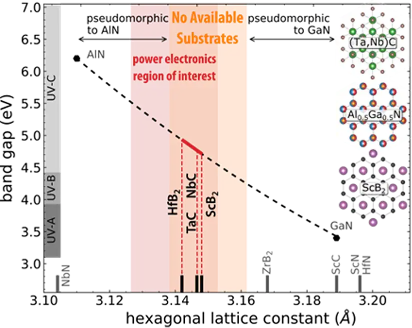
The goal of Aim 2 is to synthesize materials that remove today's "tyranny of the substrate," where achievable properties of both semiconductor materials and electronic devices are severely limited by the small subset of possible substrates. Rather than addressing just the epitaxial active layer properties, APEX also focuses on substrate and template innovation. This research is enabled by one of the few laser-heated bulk crystal growth tools, to synthesize metal diborides and carbides with metallic conductivity that could enable vertical device architectures and reduce thermal losses. These materials are ideal partners for the already established AlGaN ultra-wide bandgap material system and offer exceptional lattice and thermal expansion matching (see figure).
For more efficient, higher performance power electronics, excellent electro-thermal transport across interfaces and interface stability is needed, as well as a vertically conducting architecture to handle large currents. The primary loss mechanism in emerging high-current, vertically conducting power electronics is often resistive loss in the substrate itself. Aim 2 investigates the materials and interface science to enable solutions that significantly decrease the thermal load while simultaneously improving performance. This is accomplished by (a) targeting substrates that have metallic conductivity (>100x improvement over semiconducting silicon, SiC, or gallium nitride, GaN) and do not contribute significantly to I2R heating and (b) identifying effective methods to improve and remove the AlGaN active layer from the substrate, enabling a direct bond to the package heat sink.
Science Questions
Aim 2 is based on the related hypotheses that substrate materials exist that can fill the "lattice-matched gap" for AlGaN semiconductors (depicted below). Challenging synthesis issues with these substrates can be overcome with recent advances in floating zone bulk crystal growth, and ubstrate removal and layer transfer could enable a significant new co-design space.
Contact
For more information about the research in Aim 2 or to discuss potential collaboration, please contact Brooks Tellekamp at NLR.
Share

Last Updated Oct. 13, 2026